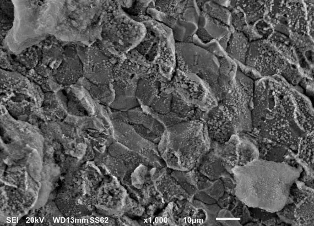

SEM - Close Up of Fracture Surface, 1000X
NTS Baltimore announces the addition of the new JOEL InTouchScopeTM JSM-6010LA Scanning Electron Microscope (SEM) with fully integrated expanded EDS (energy dispersive X-ray analyzer).

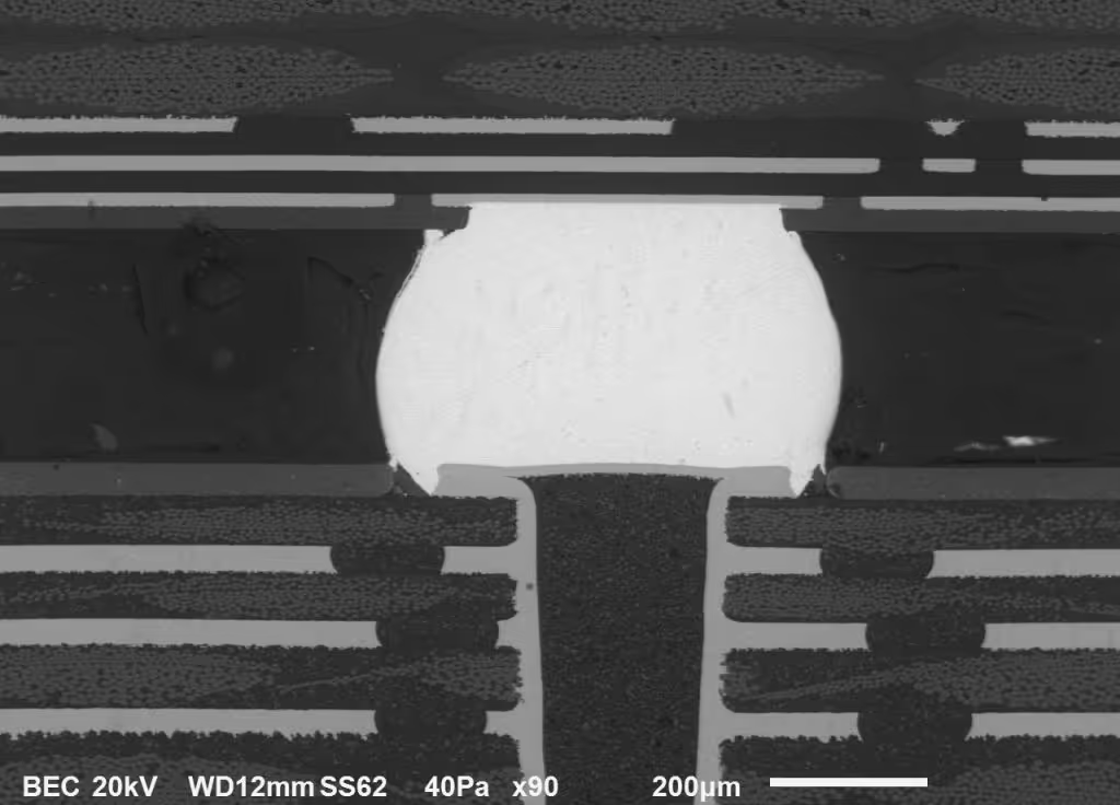
SEM - Overview of BGA Solder Joint, 90X
This research-grade SEM provides high resolution imaging and a range of acceleration voltages in both high and low vacuum modes. The embedded JEOL EDS system with silicon drift detector technology now includes spectral mapping, multi-point analysis, automatic drift compensation, partial area, line scan, and mapping filter functions. Additionally, the JSM-6010A features simultaneous multiple live image abilities that allows the client to view images remotely with magnifications from 5X – 300,000X.

SEM - Overview of Surface Pitting, 400X
“This new “live” capability will allow NTS to work more closely with our clients, allowing them real time access to their analysis from the comfort of their office”, stated Keith Sellers, Operations Manager at NTS Baltimore, adding, “From there, the client can provide immediate instruction as to how the analysis can be focused or how the analysis can be changed to meet their specific need”.Learn more about the SEM/EDS Analytical Services on our main website or contact us today to discuss your next program.